 Solar research is a hot topic the world over, with researchers working to create the next generation of solar panels. One design being explored pairs a thin, transparent network of carbon nanotubes with a layer of silicon. In this device, light passes through the transparent carbon nanotube layer to be absorbed by the silicon layer before both the silicon layer and the network of carbon nanotubes transport the generated electricity through the device.
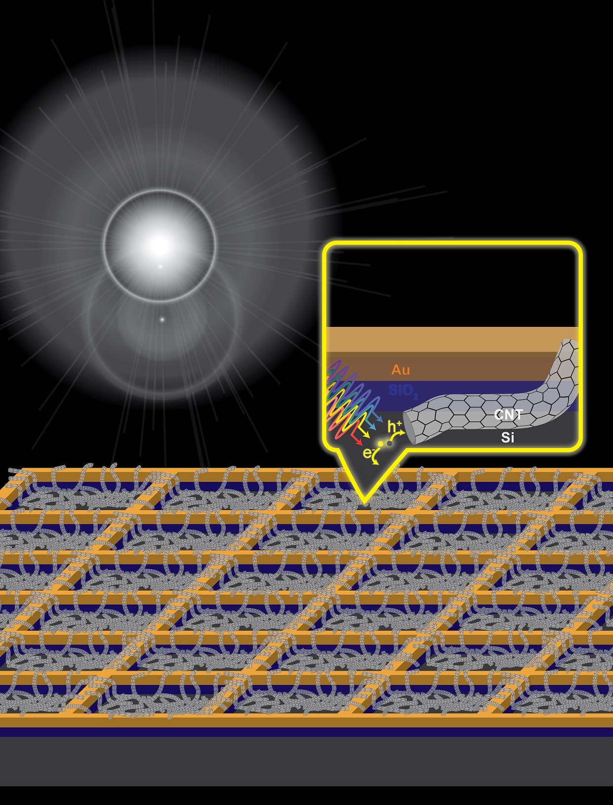
Research over the past five years has seen variations of this design achieve efficiencies of up to 17% but the commercialisation of these solar cells is hampered by significant efficiency losses at larger scales. Some have reported efficiencies approximately halving (from from 8.26% to 3.97%) as the devices were scaled up, due in part to the limited conductivity of the network of carbon nanotubes which lay on top of the silicon. Previous answers to this problem have employed a more dense network of carbon nanotubes, but this also hampers the amount of light which can make it through to be absorbed by the silicon layer underneath.
Researchers from the Centre for NanoScale Science and Technology, working under Professor Joe Shapter, have taken a new approach to solving this problem, inspired by the silicon-based solar panels which are currently sold. Their design employs a grid of gold electrodes on top of the silicon layer, keeping individual networks of nanotubes small while allowing the total device area to be increased dramatically. Their research suggests this technique may be a way to achieve large scale devices with efficiencies above 10%, previously unheard of for this style of device.
This research has also been highlighted on Advanced Science News, or you can read the full article published in Solar-RRL.